- 您现在的位置:买卖IC网 > Sheet目录2006 > LTC2494IUHF#TRPBF (Linear Technology)IC ADC 16BIT W/PGA 38-QFN
LTC2494
2494fd
applications inForMation
External Serial Clock, 3-Wire I/O
This timing mode uses a 3-wire serial I/O interface. The
conversion result is shifted out of the device by an exter-
nally generated serial clock (SCK) signal (see Figure 8).
CS is permanently tied to ground, simplifying the user
interface or isolation barrier.
The external serial clock mode is selected at the end of
the power-on reset (POR) cycle. The POR cycle is typically
concluded 4ms after VCC exceeds 2V. The level applied to
SCK at this time determines if SCK is internally generated
or externally applied. In order to enter the external SCK
mode, SCK must be driven LOW prior to the end of the
POR cycle.
Since CS is tied LOW, the end-of-conversion (EOC) can be
continuously monitored at the SDO pin during the convert
and sleep states. EOC may be used as an interrupt to an
external controller. EOC = 1 while the conversion is in
progress and EOC = 0 once the conversion is complete.
On the falling edge of EOC, the conversion result is load-
ing into an internal static shift register. The output data
can now be shifted out the SDO pin under control of the
externally applied SCK signal. Data is updated on the fall-
ing edge of SCK. The input data is shifted into the device
through the SDI pin on the rising edge of SCK. On the
24th falling edge of SCK, SDO goes HIGH, indicating a
new conversion has begun. This data now serves as EOC
for the next conversion.
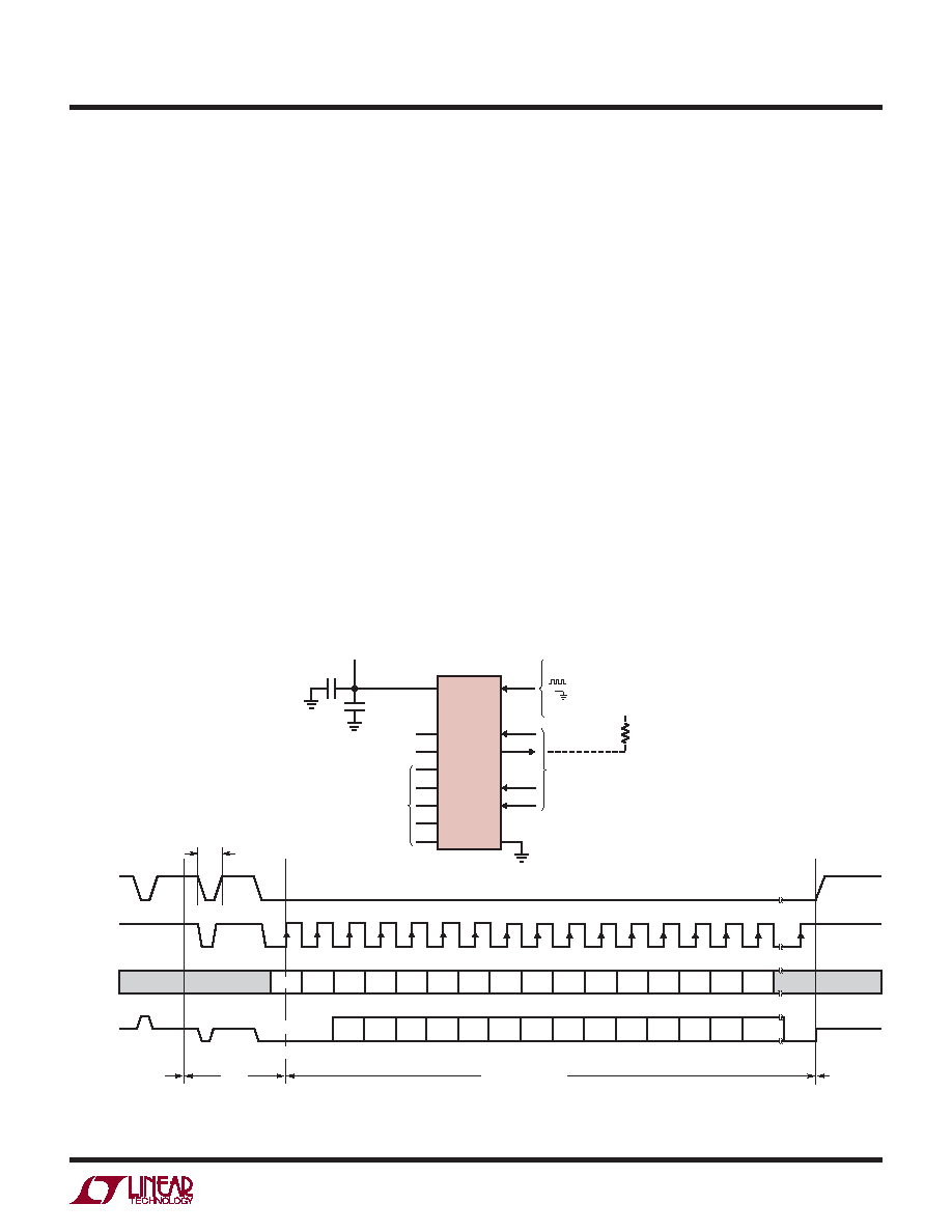
Internal Serial Clock, Single Cycle Operation
This timing mode uses the internal serial clock to shift out
the conversion result and CS to monitor and control the
state of the conversion cycle (see Figure 9).
In order to select the internal serial clock timing mode,
the serial clock pin (SCK) must be floating or pulled HIGH
before the conclusion of the POR cycle and prior to each
fallingedgeofCS.Aninternalweakpull-upresistorisactive
on the SCK pin during the falling edge of CS; therefore,
the internal SCK mode is automatically selected if SCK is
not externally driven.
Figure 9. Internal Serial Clock, Single Cycle Operation
10F
0.1F
2.7V TO 5.5V
Hi-Z
2494 F09
CS
SCK
(INTERNAL)
SDI
SDO
CONVERSION
SLEEP
DATA INPUT/OUTPUT
CONVERSION
VCC
fO
REF+
REF–
CH0
CH7
CH8
CH15
COM
SCK
SDI
SDO
CS
GND
28
35
29
30
8
15
16
23
7
38
37
1,3,4,5,6,31,32,33,39
36
34
REFERENCE
VOLTAGE
0.1V TO VCC
ANALOG
INPUTS
= EXTERNAL OSCILLATOR
= INTERNAL OSCILLATOR
LTC2494
4-WIRE
SPI INTERFACE
EOC
BIT 20 BIT 19 BIT 18 BIT 17 BIT 16 BIT 15 BIT 14 BIT 13 BIT 12 BIT 11
BIT 21
BIT 22
BIT 23
BIT 10 BIT 9
BIT 0
1
2
3
4
5
6
7
8
9
10
11
12
13
14
15
16
24
1
0
EN
SGL
A2
A1
A0
EN2
IM
FA
FB
SPD
GS2
GS1
GS0
ODD
DON'T CARE
MSB
SIG
“0”
OPTIONAL
10k
VCC
<tEOCTEST
发布紧急采购,3分钟左右您将得到回复。
相关PDF资料
LTC2495CUHF#PBF
IC ADC 16BIT W/PGA 38-QFN
LTC2496IUHF#TRPBF
IC ADC 16BIT DELTA SIG 38-QFN
LTC2498IUHF#TRPBF
IC ADC 24BIT 16CH 38-QFN
LTC2600IUFD#PBF
IC DAC OCTAL R-R 16BIT 20-QFN
LTC2602IMS8#TRPBF
IC DAC 16BIT DUAL R-R VOUT 8MSOP
LTC2604IGN-1#TRPBF
IC DAC 16BIT QUAD R-R OUT 16SSOP
LTC2605IGN-1#TRPBF
IC DAC 16BIT OCT I2C 16-SSOP
LTC2606IDD#TRPBF
IC DAC 16BIT I2C V-OUT 10-DFN
相关代理商/技术参数
LTC2495CUHF
制造商:Linear Technology 功能描述:ADC Single Delta-Sigma 15sps 16-bit Serial 38-Pin QFN EP
LTC2495CUHF#PBF
功能描述:IC ADC 16BIT W/PGA 38-QFN RoHS:是 类别:集成电路 (IC) >> 数据采集 - 模数转换器 系列:- 标准包装:1,000 系列:- 位数:16 采样率(每秒):45k 数据接口:串行 转换器数目:2 功率耗散(最大):315mW 电压电源:模拟和数字 工作温度:0°C ~ 70°C 安装类型:表面贴装 封装/外壳:28-SOIC(0.295",7.50mm 宽) 供应商设备封装:28-SOIC W 包装:带卷 (TR) 输入数目和类型:2 个单端,单极
LTC2495CUHF#TRPBF
功能描述:IC ADC 16BIT W/PGA 38-QFN RoHS:是 类别:集成电路 (IC) >> 数据采集 - 模数转换器 系列:- 标准包装:2,500 系列:- 位数:16 采样率(每秒):15 数据接口:MICROWIRE?,串行,SPI? 转换器数目:1 功率耗散(最大):480µW 电压电源:单电源 工作温度:-40°C ~ 85°C 安装类型:表面贴装 封装/外壳:38-WFQFN 裸露焊盘 供应商设备封装:38-QFN(5x7) 包装:带卷 (TR) 输入数目和类型:16 个单端,双极;8 个差分,双极 配用:DC1011A-C-ND - BOARD DELTA SIGMA ADC LTC2494
LTC2495IUHF#PBF
功能描述:IC ADC 16BIT W/PGA 38-QFN RoHS:是 类别:集成电路 (IC) >> 数据采集 - 模数转换器 系列:- 标准包装:1 系列:microPOWER™ 位数:8 采样率(每秒):1M 数据接口:串行,SPI? 转换器数目:1 功率耗散(最大):- 电压电源:模拟和数字 工作温度:-40°C ~ 125°C 安装类型:表面贴装 封装/外壳:24-VFQFN 裸露焊盘 供应商设备封装:24-VQFN 裸露焊盘(4x4) 包装:Digi-Reel® 输入数目和类型:8 个单端,单极 产品目录页面:892 (CN2011-ZH PDF) 其它名称:296-25851-6
LTC2495IUHF#TRPBF
功能描述:IC ADC 16BIT W/PGA 38-QFN RoHS:是 类别:集成电路 (IC) >> 数据采集 - 模数转换器 系列:- 标准包装:1,000 系列:- 位数:16 采样率(每秒):45k 数据接口:串行 转换器数目:2 功率耗散(最大):315mW 电压电源:模拟和数字 工作温度:0°C ~ 70°C 安装类型:表面贴装 封装/外壳:28-SOIC(0.295",7.50mm 宽) 供应商设备封装:28-SOIC W 包装:带卷 (TR) 输入数目和类型:2 个单端,单极
LTC2496CUHF#PBF
功能描述:IC ADC 16BIT DELTA SIG 38-QFN RoHS:是 类别:集成电路 (IC) >> 数据采集 - 模数转换器 系列:- 标准包装:1 系列:microPOWER™ 位数:8 采样率(每秒):1M 数据接口:串行,SPI? 转换器数目:1 功率耗散(最大):- 电压电源:模拟和数字 工作温度:-40°C ~ 125°C 安装类型:表面贴装 封装/外壳:24-VFQFN 裸露焊盘 供应商设备封装:24-VQFN 裸露焊盘(4x4) 包装:Digi-Reel® 输入数目和类型:8 个单端,单极 产品目录页面:892 (CN2011-ZH PDF) 其它名称:296-25851-6
LTC2496CUHF#TRPBF
功能描述:IC ADC 16BIT DELTA SIG 38-QFN RoHS:是 类别:集成电路 (IC) >> 数据采集 - 模数转换器 系列:- 标准包装:2,500 系列:- 位数:16 采样率(每秒):15 数据接口:MICROWIRE?,串行,SPI? 转换器数目:1 功率耗散(最大):480µW 电压电源:单电源 工作温度:-40°C ~ 85°C 安装类型:表面贴装 封装/外壳:38-WFQFN 裸露焊盘 供应商设备封装:38-QFN(5x7) 包装:带卷 (TR) 输入数目和类型:16 个单端,双极;8 个差分,双极 配用:DC1011A-C-ND - BOARD DELTA SIGMA ADC LTC2494
LTC2496IUHF#PBF
功能描述:IC ADC 16BIT DELTA SIG 38-QFN RoHS:是 类别:集成电路 (IC) >> 数据采集 - 模数转换器 系列:- 标准包装:2,500 系列:- 位数:16 采样率(每秒):15 数据接口:MICROWIRE?,串行,SPI? 转换器数目:1 功率耗散(最大):480µW 电压电源:单电源 工作温度:-40°C ~ 85°C 安装类型:表面贴装 封装/外壳:38-WFQFN 裸露焊盘 供应商设备封装:38-QFN(5x7) 包装:带卷 (TR) 输入数目和类型:16 个单端,双极;8 个差分,双极 配用:DC1011A-C-ND - BOARD DELTA SIGMA ADC LTC2494